Advanced Digital Design Concepts (Real Problems)
1) Below is a Top level block diagram of a Design. What could be the problem with this Design?
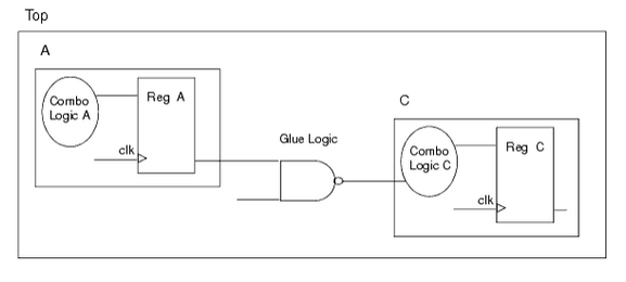
Ans - The above circuit diagram shows an invalid design where a NAND gate exists at the top level, between two lower-level design blocks. Optimization is limited because synthesis tools such as Design Compiler cannot merge the NAND with the combinational logic inside block C.

The above diagram shows a valid similar design where the NAND gate is included as part of the combinational logic in block C. This approach eliminates the extra CPU cycles needed to compile small amounts of glue logic and provides for simpler synthesis script development. An automated script mechanism only needs to compile and characterize the leaf-level cells.
2) What could be the problem with below code snippet ?
module myModule_BAD (DATA_IN, DATA_OUT, A); input [7:0] DATA_IN; input [3:0] A; output [7:0] DATA_OUT; assign DATA_OUT = (DATA_IN << A); endmodule
Ans - The shift value must be an expression that can be evaluated at compilation or elaboration time. A shift by a dynamic value results in a huge combinatorial area. If the shift value can be defined at the compilation or elaboration step, the synthesis tool will only perform net assignment. Below are the valid code snippet -
Valid Verilog Code:
module myModule_GOOD1 (DATA_IN, DATA_OUT); input [7:0] DATA_IN; output [7:0] DATA_OUT; assign DATA_OUT = (DATA_IN << 3 ); // Shift value is constant (literal) endmodule
Valid Verilog code:
module myModule_GOOD2 (data_in, data_out); input [7:0] data_in ; output [7:0] data_out; parameter n = 4; assign data_out = data_in >> n; // Shift value is constant (parameter) assign data_out = data_in << n; // Shift value is constant (parameter) endmodule
3) Find out the issue with below code snippet ?
module myModule_BAD (A, B, SEL, DATA_OUT); input A, B, SEL; output DATA_OUT; reg DATA_OUT; always@(A or B or SEL) begin if (SEL === 1'bX) DATA_OUT <= A; else DATA_OUT <= B; end endmodule
Ans - Operators , "===" and "!==" in HDL source cannot be synthesized.
4) What could be the problem with below circuit diagram ?
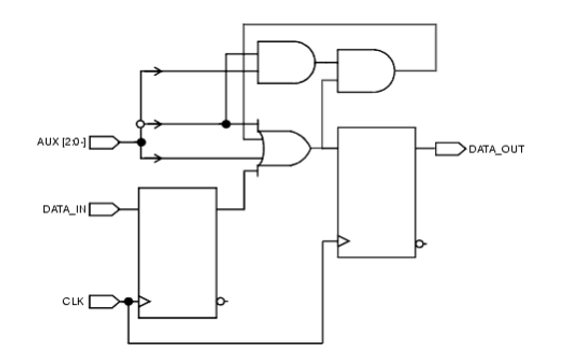
Ans - The above circuit diagram illustrates an asynchronous feedback loop in a design. Asynchronous feedback loops can create instability in design.
5) Why Latches (Inferred or Instantiated {e.g in .db libraries}) are not recommended in Design ?
Ans - Latches are generally not recommended because they cause problems with scan insertion and timing analysis.
The following examples show poor and recommended coding styles if you need to use latches in your design
Poor coding style: latch inferred because of missing else condition-
EX21_PROC: process (a, b) begin if (a = '1') then q <= b; end if; end process EX21_PROC;
Poor coding style: latch inferred because of missing z output assignment-
library IEEE; use IEEE.std_logic_1164.all; use IEEE.std_logic_arith.all; use IEEE.STD_LOGIC_UNSIGNED.conv_integer; entity c_1003 is port ( c : in std_logic; q , z : out std_logic ); end; architecture arch of c_1003 is begin EX22_PROC: process (c) begin case c is when '0' => q <= '1'; z <= '0'; when others => q <= '0'; end case; end process EX22_PROC; end architecture;
Poor coding style: latches inferred because of missing 's' output assignments for the 2'b00 and 2'b01 conditions and a missing 2'b11 condition-
always @ (d) begin case (d) 2'b00: z <= 1'b1; 2'b01: z <= 1'b0; 2'b10: z <= 1'b1; s <= 1'b1; endcase end
Guideline - You can avoid inferred latches by using any of the following coding techniques:
Assign default values at the beginning of a process, as shown for VHDL in Example A.
Assign outputs for all input conditions, as shown in Example B.
Use else (instead of elsif) for the final priority branch, as shown in Example C.
Example A. Avoiding a latch by assigning default values.
COMBINATIONAL_PROC : process (state, bus_request) begin -- intitialize outputs to avoid latches bus_hold <= '0'; bus_interrupt <= '0' case (state) ... ................. ................. end process COMBINATIONAL_PROC;
Example B. Avoiding a latch by fully assigning outputs for all input conditions.
Poor coding style:
EX25A_PROC: process (g, a, b) begin if (g = '1') then q <= 0; elsif (a = '1') then q <= b; end if; end process EX25A_PROC;
Recommended coding style:
EX25B_PROC: process (g1, g2, a, b) begin q <= '0'; if (g1 = '1') then q <= a; elsif (g2 = '1') then q <= b; end if; end process EX25B_PROC;
Example C. Avoiding a latch by using else for the final priority branch (VHDL).
Poor coding style:
MUX3_PROC: process (decode, A, B) begin if (decode = '0') then C <= A; elsif (decode = '1') then C <= B; end if; end process MUX3_PROC;
Recommended coding style:
MUX3_PROC: process (decode, A, B) begin if (decode = '1') then C <= A; else C <= B; end if; end process MUX3_PROC;
---------------------------------------------------Happy Learning--------------------------------------
module myModule_GOOD2 (data_in, data_out); input [7:0] data_in ; output [7:0] data_out; parameter n = 4; assign data_out = data_in >> n; // Shift value is constant (parameter) assign data_out = data_in << n; // Shift value is constant (parameter) endmodule
3) Find out the issue with below code snippet ?
module myModule_BAD (A, B, SEL, DATA_OUT); input A, B, SEL; output DATA_OUT; reg DATA_OUT; always@(A or B or SEL) begin if (SEL === 1'bX) DATA_OUT <= A; else DATA_OUT <= B; end endmodule
Ans - Operators , "===" and "!==" in HDL source cannot be synthesized.
4) What could be the problem with below circuit diagram ?
Ans - The above circuit diagram illustrates an asynchronous feedback loop in a design. Asynchronous feedback loops can create instability in design.
5) Why Latches (Inferred or Instantiated {e.g in .db libraries}) are not recommended in Design ?
Ans - Latches are generally not recommended because they cause problems with scan insertion and timing analysis.
The following examples show poor and recommended coding styles if you need to use latches in your design
Poor coding style: latch inferred because of missing else condition-
EX21_PROC: process (a, b) begin if (a = '1') then q <= b; end if; end process EX21_PROC;
Poor coding style: latch inferred because of missing z output assignment-
library IEEE; use IEEE.std_logic_1164.all; use IEEE.std_logic_arith.all; use IEEE.STD_LOGIC_UNSIGNED.conv_integer; entity c_1003 is port ( c : in std_logic; q , z : out std_logic ); end; architecture arch of c_1003 is begin EX22_PROC: process (c) begin case c is when '0' => q <= '1'; z <= '0'; when others => q <= '0'; end case; end process EX22_PROC; end architecture;
Poor coding style: latches inferred because of missing 's' output assignments for the 2'b00 and 2'b01 conditions and a missing 2'b11 condition-
always @ (d) begin case (d) 2'b00: z <= 1'b1; 2'b01: z <= 1'b0; 2'b10: z <= 1'b1; s <= 1'b1; endcase end
Guideline - You can avoid inferred latches by using any of the following coding techniques:
Assign default values at the beginning of a process, as shown for VHDL in Example A.
Assign outputs for all input conditions, as shown in Example B.
Use else (instead of elsif) for the final priority branch, as shown in Example C.
Example A. Avoiding a latch by assigning default values.
COMBINATIONAL_PROC : process (state, bus_request) begin -- intitialize outputs to avoid latches bus_hold <= '0'; bus_interrupt <= '0' case (state) ... ................. ................. end process COMBINATIONAL_PROC;
Example B. Avoiding a latch by fully assigning outputs for all input conditions.
Poor coding style:
EX25A_PROC: process (g, a, b) begin if (g = '1') then q <= 0; elsif (a = '1') then q <= b; end if; end process EX25A_PROC;
Recommended coding style:
EX25B_PROC: process (g1, g2, a, b) begin q <= '0'; if (g1 = '1') then q <= a; elsif (g2 = '1') then q <= b; end if; end process EX25B_PROC;
Example C. Avoiding a latch by using else for the final priority branch (VHDL).
Poor coding style:
MUX3_PROC: process (decode, A, B) begin if (decode = '0') then C <= A; elsif (decode = '1') then C <= B; end if; end process MUX3_PROC;
Recommended coding style:
MUX3_PROC: process (decode, A, B) begin if (decode = '1') then C <= A; else C <= B; end if; end process MUX3_PROC;
---------------------------------------------------Happy Learning--------------------------------------


You've written a very useful article. This article provided me with some useful knowledge. Thank you for providing this information. Keep up the good work. vlsi courses in bangalore
ReplyDelete