Thursday, July 22, 2021

Verilog HDL Examples - Design of Gray Code Counter (For FIFO Design)


Gray Code :

- Named after Frank Gray

- Known as reflected binary code (RBC),

- Also known just as reflected binary (RB) or Gray Code

- An ordering of the binary numeral system such that two successive values differ in only one bit (binary digit)

Decimal(Base 10) Binary (Base 2) Binary Reflected/Gray (No Base)

0 0000 0000

1 0001 0001

2 0010 0011

3 0011 0010

4 0100 0110

5 0101 0111

6 0110 0101

7 0111 0100

-----------------------------------------------------------------------------------------------------------------------------

8 1000 1100

9 1001 1101

10 1010 1111

11 1011 1110

12 1100 1010

13 1101 1011

14 1110 1001

15 1111 1000


- The second half of the 4 bit gray code counter is the mirror image of the first half of the gray code counter with the MSB inverted

- By inverting the 2nd MSB of the second half of the 4-bit gray code will produce the 3-bit Gray code sequence in the 3 LSBs of the 4 bit Gray code

- The 3-bit Gray code with the MSB is no longer a true Gray code because when the sequence changes from 7 to 8 or 15 to 0 , two bits are changing instead of just one bit


- Below is the circuit diagram to generate n-bit and (n-1) bit Gray code counter


- This circuit assumes that the register output is a Gray Code value itself

- Top half of the above circuit diagram shows n bit Gray code while the bottom shows (n-1) bit Gray Code Logic


-------------------------Happy Learning ----------------------------

Data-To-Data [Non-Sequential] Timing Checks


Data To Data Timing Checks :

- Setup and hold checks between two data pins (neither of these is defined as a clock)

- Also referred as Non-Sequential Constraints

- One data pin is the constraint pin , like a data pin of a flop and the second pin is the related pin which acts like a clock pin of a flop

- Below is the circuit diagram -


- This check is useful in a design where it may be necessary to provide specific arrival times of one signal with respect to other

- The Data-To-Data setup check is performed on the same clock edge as the launch edge

- Hence, this check is also known as zero-cycle check or same-cycle check

- Specifying Data-To-Data or Non-Sequential Check - Constrains can be defined in the timing library (.lib model) for a cell or can be set interactively using the set_data_check command in SDC

1) Non-Sequential check defined in the timing library -

pin ( D1 ) {

direction : input;
timing ( )
related_pin : “D2";
timing_type : non_seq_setup_rising;

...

timing ( )
related_pin : “D2";
timing_type : non_seq_hold_falling;

2) Data-To-Data Check defined by SDC Command -

set_data_check –rise_from D2 –to D1 –setup <x> set_data_check –fall_from D2 –to D1 –hold <y>

- if signals are coming from different clock domains -

set_data_check –rise_from D2 –to D1 –setup <x> -clock clockA

set_data_check –fall_from D2 –to D1 –hold <y> -clock clockA

Note : 'x' and 'y ' are setup and hold time values

Difference between Non-Sequential Check and Data-To-Data Check -

1) The setup and hold values are obtained from the timing library for Non-Sequential check where the setup and hold timing models are described. In a Data-To-Data check only a single value can be specified for the setup and hold check.

2) Non-Sequential checks in .lib are more accurate since it is sensitive to the slew of constrained and related pin

3) Non-Sequential check can only be applied to the pins of a cell, whereas a Data-To-Data check can be applied to any two arbitrary pins in a design


Note : In case Data -To-Data checks are specified through the library as well as with the set_data_check command interactively, then the value specified by set_data_check will be used for the Data-To-Data check.


Example :

set_data_check -from D2 -to D1 -setup 2.1

set_data_check -from D2 -to D1 -hold 1.5


- Setup data check implies that D1 should arrive at-least 2.1ns prior to the edge of the related pin D2 , otherwise it is a Data-To-Data setup check violation.

- Hold data check specifies that D1 should arrive at-least 1.5ns after D2. If the constrained signal arrive earlier than this specification, then it is a Data-To-Data hold check violation.


------------------------------------------------------Happy Learning------------------------------------


Wednesday, July 21, 2021

Verilog HDL Examples - FIFO Design - Asynchronous FIFOs


Asynchronous FIFO Design :

- A FIFO Design where data values are written to a FIFO buffer from one clock domain and the data values are read from the same FIFO buffer from another clock domain

- The clock domain are asynchronous to each other

- Asynchronous FIFOs are used to safely pass the data from one clock domain to another clock domain

- The main difficulty in designing the asynchronous FIFO design is related to generating the FIFO

pointers and finding a reliable way to determine FULL and EMPTY status on the FIFO

- Unlike synchronous FIFO Design (here) , the increment -decrement FIFO fill counter can not be used because two different and asynchronous clocks would be required to control the counter

- We need to compare write and read pointers to determine full and empty status for an asynchronous FIFO design

- The FIFO is empty when both read and write pointers are equal which happens when both pointers are reset to zero during a reset operation or when the read pointer catches up to the write pointer , having read the last word from the FIFO

- The FIFO is full when both write and read pointers are again equal that is when the write pointer has wrapped around and caught up to the read pointer

- In both Empty and Full FIFO condition both read and write pointers are equal. Problem ? Yes definitely ... Lets see how this can be avoided -

- Add an extra bit to each pointer

- When the write pointer increments past the final FIFO address, the write pointer will increment the unused MSB bit while setting rest of the bits to zero. The same is done for the read pointer.

- If the MSB of the two pointers are different, that means the write pointer has wrapped one more time than the read pointer

- If the MSB of both pointers are same that means both pointers have wrapped the same number of times


- EMPTY : When both read and synchronized write pointers are equal including MSB bit

- FULL : When the MSB is different and rest of the bits of both pointers are same

- Trying to synchronize a binary count value from one clock domain to another is problematic because every bit of an N-bit counter can change simultaneously ( Ex. 7 [0111] -> 8[1000])

- A good approach for FIFO counter pointers is to use Gray code counter. They allow only one bit to change for every clock transaction , eliminating the problem associated with trying to synchronize multiple changing signals on the same clock edge

- Block diagram of an Asynchronous FIFO -


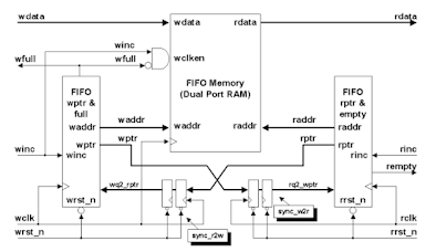
- The write and read pointers are synchronized in the other domain before they are used for the comparison

- In this FIFO architecture, the read and write pointer must be passed to the opposite clock domain for pointer comparison

- There is a problem using Gary Code for determining the FULL condition as the Gray code is a symmetric code except the MSB bit 


- Problem #1 : As depicted in the above picture when both pointers points to the location Gray-7(The FIFO is EMPTY ) , On the next write operation, writer pointer will increment the Gray Counter and will point to (1_100) where the MSB of read and write pointer are not same but rest of the bits are same and the FIFO FULL Flag will get asserted which is WRONG ( Read Pointer = 0_100 , Write Pointer = 1_100)

- Problem #2 : When the write counter increments from Gray 7 to Gray 8, the 3 bit MSB ( which really points the memory address) are unchanged and results in the same memory location over- write

- Solution : Synchronized the read pointer in write clock domain and then meet the below 3 necessary conditions to calculate the FIFO FULL condition -

1) Write pointer and synchronized read pointers MSB's must be unequal ( Ensures one more time write pointer wrapping )

2) Write pointer and synchronized read pointer's MSB's are not equal (Use (n-1) Gray Code as discussed previously , the inverted 2nd MSB of write pointer must be tested against the un-inverted 2nd MSB's of read pointer )

3) All other bits of write and read pointer must be equal


Verilog HDL Code:

// Code your design here

module async_fifo #(parameter FIFO_DEPTH = 8,
parameter DATA_WIDTH = 8)(
input w_clk,
input r_clk,
input rst,
input [7:0] w_data,
input w_en,
output [7:0] r_data,
input r_en,
output full,
output empty
);

reg [3:0] wr_ptr, rd_ptr, wr_ptr_synced, rd_ptr_synced; // Extra 1 bit MSB for 'full' condition check
reg [3:0] wr_ptr_g, rd_ptr_g;
reg [DATA_WIDTH-1:0] mem[0: FIFO_DEPTH -1];

assign full = ((wr_ptr_synced[2:0] == rd_ptr_synced[2:0]) && (wr_ptr_synced[3] != rd_ptr_synced[3]));
assign empty = (wr_ptr_synced == rd_ptr_synced);

always @(posedge w_clk)
begin
if(w_en && !full)
begin
mem[wr_ptr] <= w_data;
end
end

always @(posedge r_clk)
begin
if(r_en && !empty)
begin
r_data <= mem[rd_ptr];
end
end

always @(posedge w_clk or negedge rst)
begin
if(!rst)
begin
wr_ptr <= 4'b0;
end
else if(w_en)
begin
wr_ptr <= wr_ptr + 1;
end
end

always @(posedge r_clk or negedge rst)
begin
if(!rst)
begin
rd_ptr <= 4'b0;
end
else if(r_en)
begin
rd_ptr <= rd_ptr + 1;
end
end

binary2gray b2g_wr_ptr(.i_binary(wr_ptr), .o_gray(wr_ptr_g)); //Not used here , Any Challenge if using gray code?
binary2gray b2g_rd_ptr(.i_binary(rd_ptr), .o_gray(rd_ptr_g)); // Not used here ,Any Challenge if using gray code?

dff_sync2 dff_sync2_wr_ptr_0(.clk(r_clk), .rst(rst), .d(wr_ptr[0]), .q_synced(wr_ptr_synced[0]));
dff_sync2 dff_sync2_wr_ptr_1(.clk(r_clk), .rst(rst), .d(wr_ptr[1]), .q_synced(wr_ptr_synced[1]));
dff_sync2 dff_sync2_wr_ptr_2(.clk(r_clk), .rst(rst), .d(wr_ptr[2]), .q_synced(wr_ptr_synced[2]));
dff_sync2 dff_sync2_wr_ptr_3(.clk(r_clk), .rst(rst), .d(wr_ptr[3]), .q_synced(wr_ptr_synced[3]));
dff_sync2 dff_sync2_rd_ptr_0(.clk(w_clk), .rst(rst), .d(rd_ptr[0]), .q_synced(rd_ptr_synced[0]));
dff_sync2 dff_sync2_rd_ptr_1(.clk(w_clk), .rst(rst), .d(rd_ptr[1]), .q_synced(rd_ptr_synced[1]));
dff_sync2 dff_sync2_rd_ptr_2(.clk(w_clk), .rst(rst), .d(rd_ptr[2]), .q_synced(rd_ptr_synced[2]));
dff_sync2 dff_sync2_rd_ptr_3(.clk(w_clk), .rst(rst), .d(rd_ptr[3]), .q_synced(rd_ptr_synced[3]));

endmodule

module binary2gray #(NUM_BITS = 4)(
input[3:0] i_binary,
output[3:0] o_gray
)

assign o_gray[3] = i_binary[3];
assign o_gray[2] = i_binary[3] ^ i_binary[2];
assign o_gray[1] = i_binary[2] ^ i_binary[1];
assign o_gray[0] = i_binary[1] ^ i_binary[0];

endmodule


module dff_sync2(
input clk,
input rst,
input d,
output q_synced
);

reg sync_flop1;
reg sync_flop2;

always @(posedge clk or negedge rst)
begin
if(!rst)
begin
sync_flop1 <= 1'b0;
sync_flop2 <= 1'b0;
end
else begin
sync_flop1 <= d;
sync_flop2 <= sync_flop1;
end
end
assign q_synced = sync_flop2;
endmodule


-------------------------------------------------Happy Learning -----------------------------------------

Verilog HDL Examples - FIFO Design - Synchronous FIFOs


Synchronous FIFO Design :

Lets have a look at below block diagram of Synchronous FIFO. Further we will have a look at its Verilog HDL implementation.


For synchronous FIFO design (a FIFO where writes to, and reads from the FIFO buffer are conducted in the same clock domain), one implementation counts the number of writes to, and reads from the FIFO buffer to increment (on FIFO write but no read), decrement (on FIFO read but no write) or hold (no writes and reads, or simultaneous write and read operation) the current fill value of the FIFO buffer. The FIFO is full when the FIFO counter reaches a predetermined full value and the FIFO is empty when the FIFO counter is zero.

Lets assume a FIFO with 8 words depth.


//Generation of Empty and Full Conditions

---------------------------------------------------------------------------------------------------

Module fifo(

input [7:0] data_in,

input clk,

input rst , rd, wr,

output empty, full ,

output reg [3:0] fifo_cnt,

output reg[7:0] data_out);

reg [7:0] fifo_ram[0:7];

reg [2:0] rd_ptr, wr_ptr;

assign empty = (fifo_cnt == 0);

assign full = (fifo_cnt == 8);

------------------------------------------------------------------------------------------------------

// fifo_ram writing & reading

------------------------------------------------------------------------------------------------------

always @(posedge clk) begin : WRITE

if(wr && !full)

fifo_ram[wr_ptr] = data_in;

else if (wr && rd)

fifo_ram[wr_ptr] = data_in;

end

always @(posedge clk) begin : READ

if(rd && !empty)

data_out = fifo_ram[rd_ptr];

else if (rd && wr)

data_out = fifo_ram[rd_ptr];

end

--------------------------------------------------------------------------------------------------------

//Pointer Generation

--------------------------------------------------------------------------------------------------------

always @ (posedge clk) begin : POINTER

if (rst) begin

wr_ptr <= 0;

rd_ptr <= 0;

end

else if begin

wr_ptr <= ((wr && !full) || (wr && rd)) ? wr_ptr + 1 : wr_ptr;

rd_ptr <= ((rd && !empty) || (rd && wr)) ? rd_ptr +1 : rd_ptr;

end

end

---------------------------------------------------------------------------------------------------------

//Counter Logic Generation

---------------------------------------------------------------------------------------------------------

always @ (posedge clk) begin : COUNTER

if (rst)

fifo_cnt <= 0;

else begin

case ((wr, rd))

2'b00 : fifo_cnt <= fifo_cnt;

2'b01 : fifo_cnt <= (fifo_cnt == 0) ? 0 : fifo_cnt - 1;

2'b10 : fifo_cnt <= (fifo_cnt == 8) ? 8 : fifo_cnt + 1;

2'b11 : fifo_cnt <= fifo_cnt;

default : fifo_cnt <= fifo_cnt;

endcase

end

end

-------------------------------------------------------------------------------------------------------


Timing Diagram : (FIFO Depth = 4)


Happy Learning !!!


Monday, July 19, 2021

Bluetooth Low Energy - Link Layer Hardware Design : Architecture Overview


Link Layer Hardware Architecture :

Lets have a look at the complete Bluetooth Low Energy (BLE) Stack Diagram below. Here, Application and Host of the BLE Stack are Software/Firmware component while Controller is a Hardware component. We will be focusing on the implementation of Link Layer (LL) subcomponent of the controller hardware in this series of blog post.


Figure#1 : BLE Stack Block Diagram

Now, Lets see the various sub-components of Link Layer Hardware as depicted in the below block diagram. We will be discussing each and every component in details throughout this blog series and how they can be designed/implemented using HDL.


Figure#2 : Link Layer Hardware Architecture Diagram


The main functionality of Bluetooth Low Energy Link Layer Hardware includes -

- Control and manage all advertising procedures of all types of advertising packets

- Manages scan procedures including passive and active scanning

- Manages whitelist and duplicate filtering polices of BLE Stack

- Manages and controls connection procedures both as a Master and a Slave

- Link Sustenance (After a BLE connection is established between a Master and Slave)

- Controls and manages Link supervision timeout

- Manages Connection update and channel map update procedures

- Transmission and Re-transmission of BLE packets

- Acknowledgement and flow control

- Bit processing of packets (CRC, data whitening )

- Framing and de-framing of packets

- Supports and interface to processor bus for updating LL Hardware registers

- Support for various power saving modes for power optimized hardware implementation

- Supports for data encryption/decryption engines

Continued - - -

Happy Learning !!!

System Verilog Assertions - Nonconsecutive Repetition


Nonconsecutive Repetition :

- Repeated, Nonconsecutive Boolean expressions can be defined using [=N]

- Nonconsecutive - Not necessarily consecutive

- Syntax : expr[=N]; expr must occur N times

- Example : When A is high then from the same cycle , there must be two cycles of B before C


property NONCONSECUTIVE_REPET;

@(negedge CLK) A |-> B[=2] ##1 C;

endproperty

assert property (NONCONSECUTIVE_REPET);


Note: In Non Consecutive Repetition Sequence , here there is no restrictions of number of cycles between second B and C.

Go-To Repetition :

- Syntax : expr[->N]

- Go to repetition operator is similar to the Nonconsecutive operator except expr must be true in the last cycle of the sequence

- Example : When A is high then from the same cycle , there must be two cycles of B before C , with C immediately following the second B


property GOTO_REPET;

@(negedge CLK) A |-> B[->2] ##1 C;

endproperty

assert property (GOTO_REPET);


Note: Last occurrence of B must be followed immediately by C


Hope, this blog post is helpful in understanding the tiny difference between these two operators while coding System Verilog Assertions.


Please like/share/comment and follow VLSI Excellence for such more interesting blog posts.


Happy Learning !!!

System Verilog Assertions - Consecutive Repetition


Consecutive Repetition :

- Repeated, consecutive sequences can be defined using [*N]

- Syntax : SEQ[*N]; SEQ, repeated N times

- Example : A is never low for more than 4 cycles


property CONSECUTIVE_REPET;

@(negedge CLK) !A[*4] |=> A;

endproperty

assert property (CONSECUTIVE_REPET);


Consecutive Repetition with Ranges :

- Syntax : SEQ[*min : max] ; SEQ will repeat from min to max times

- Example : A is low for 2 to 4 cycles only


property CONSECUTIVE_REPET_RANGE;

@(negedge CLK) A ##1 ~A |=> !A[*1:3] ##1 A;

endproperty

assert property (CONSECUTIVE_REPET_RANGE);

Consecutive Repetition - Special Range Cases :

- Lower bound can be 0

- No minimum number of repetition , sequence may be absent

- Example :

A ##1 B[*0:2] ##1C;

- Possible Sequences - (A##1 C), (A ##1B ##1 C), (A ##1 B ##1 B ##1 C)

- Lower bound can be infinity ($)

- No maximum number of repetition , sequence might never end

- Example :

A[*2:$] ##1 B

- Possible Sequences - (A ##1 A ##1 B) , (A ##1 A ##1 A ---)


--------------------------------------------------Happy Learning-----------------------------------------

Sunday, July 18, 2021

System Verilog Assertions - Sequences


System Verilog Sequences :

- Temporal properties are described using sequences

- Series of Boolean equations

- Each cycle separated by ##

- Syntax : SEQ_A |-> SEQ_B OR SEQ_A |=> SEQ_B

- Properties are either unconditional using instantaneous Boolean expression

property UNCONDITIONAL:

@(posedge CLK) (COUNT >10);

endproperty

- OR , conditional using implication operators

property CONDITIONAL;

@(posedge CLK) A |=> B ##1 C;

endproperty

- If Enabling Sequence (A) is True, than only Fulfilling Sequence (B ##1 C) will Evaluate.


Disabling Properties -

- To terminate an assertion when a condition is true

- use disable iff (expr)

- If expr is true at any point of time, then the property is terminated and it Passes.

- Useful for cancelling multicycle sequence properties

- Example :

property ABORT;

@(negedge CLK) disable iff (RST)

A |=> B ##1 C ##1 D;

endproperty

assert property (ABORT);


--------------------------------------------------------Happy Learning----------------------------------

System Verilog Assertions - Useful Built-in Functions


$past() :

- Returns the value of a signal from previous evaluation cycle

- Syntax : $past (A, N) ; Default N = 1

- Example :

property PAST1;

@(negedge CLK) EN |-> (OP == $past(IP , 2 ));

endproperty

assert property (PAST1);


$stable() :

- Returns a Boolean True value if expr has the same value as it did in the previous cycle.

- Syntax : $stable(expr)

- Example :

property STABLE;

@(negedge CLK) ~ENAB |=> $stable(DOUT);

endproperty

assert property (STABLE);


$countones() :

- Returns the number of 1's in expr

- Any value other than 1 is ignored

- Syntax : $countones(expr)

- Example :

property 1HOT_CHK;

@(negedge CLK) ($countones(B_VECTOR) == 1);

endproperty

assert property (1HOT_CHK);

$isunknown() :

- Returns a Boolean True if any bit in expr is 'x' or 'z'

- Syntax : $isunknown(expr)

- Example :

property CHK_UNKNOWN;

@(negedge CLK) (~EN |=> $isunknown(B_VECTOR));

endproperty

assert property (CHK_UNKNOWN);

- When EN is low, check that any bits of B_VECTOR is driven as 'x' OR 'z'

$onehot() :

- Returns a Boolean True only if exactly one bit in expr is 1

- Syntax : $onehot(expr)

- Example :

property ONEHOT;

@(negedge CLK) ($onehot(B_VECTOR));

end property

assert property (ONEHOT);

$onehot0() :

- Returns a Boolean True only if, at most, 1 bit in expr is 1

- Syntax : #onehot0(expr)

- Example :

property ONEHOT0;

@(negedge CLK) ($onehot0(B_VECTOR));

endproperty

assert property (ONEHOT0);


$rose() :

- Click Here

$fell() :

- Click Here


Hope, this blog post is helpful in understanding the useful System Verilog built-in functions.

Please do like/share/comment and follow VLSI Problems for such more interesting blog posts.

Happy Learning !!!

Saturday, July 17, 2021

System Verilog Assertions - Assertion Overlapping


Assertion Overlapping :

- Assertions are checked at every evaluation point.

- If the start condition is true, a new assertion is triggered.

- Many copies of an assertion may be active simultaneously.

Example :

property A0;

@(negedge CLK) REQ |=> ACK;

endproperty

assert property (A0);


Since, the REQ is still high at second negedge of CLK and it triggers an unexpected second assertion.

Note: Assertions must be carefully written to avoid unexpected failures from overlapping.

How this can be avoid OR how can you code a robust assertion ?

- Use built-in functions for detecting value change.

- $rose() and $fell()

- Useful for making properties edge triggered.

- One way to avoid overlapping - $rose(expr) - True if expr has changed value and it is 1 in the current cycle

- $fell() - True if expr has changed value and it is 0 in the current cycle

- $rose() is true for x->1 and z->1 changes

Example :

property ET;

@(negedge CLK) $rose(REQ) |=> ACK;

endproperty

assert property (ET);


Here, at second negedge of CLK , a new assertion is not getting triggered since there is no change in REQ.


Hope, this blog is helpful to understand assertion overlapping, their cons and how they can be avoided.


Please like/share/comment and follow VLSI Excellence for more such interesting blog posts.

Thanks !!!

-----------------------------------------------------Happy Learning -------------------------------------

System Verilog Assertions - Implication Operators


Same Cycle Implication ( |->) :

Only under certain conditions assertions may be valid.

exp1 |-> exp2 ;


If exp1 is true then exp2 must be true at the same evaluation point.

Example :

property SameCyImp

@(negedge CLK) (REQ && ~ACK) |-> BUSY ;

endproperty

assert property (SameCyImp);


Next Cycle Implication ( |=>) :

exp1 |=> exp2;

If exp1 is true , then exp2 must be true at the next evaluation point.

Example :

property NextCyImp

@(negedge CLK) (REQ && ~ACK) |=> BUSY;

endproperty

assert property (NextCyImp);


Hope, this blog is helpful to understand the use case of Same Cycle and Next Cycle Implication Operators clearly.


Please feel free to like/share/comment and follow VLSI Excellence for more such interesting blog posts.

Thanks !!!


-------------------------------------------------------------Happy Learning------------------------------

System Verilog Assertions - Clocked Property Evaluation


Clocked Property Evaluation :

Remember - "Objects are sampled before the Clock Edge"

Lets have a look at below examples -

1) property EN_1HOT

@(EN1 or EN2) (EN1 | EN2)

endproperty

2) property EN_1HOT_CLK

@(psoedge CLK) (EN1 | EN2)

endproperty

Now, Lets have a look at the signal waveform below -


Important Points:


1) EN_1HOT Property is evaluated whenever there is a change in EN1 or EN2 Signal ( As shown in above waveform)

2) EN_1HOT_CLK Property is evaluated at every Positive Edge of the Clock ( As shown in above waveform)

3) As you observe in the above waveform when a property evaluates, the property expression objects are evaluated before the property clocking expression ( See the point in the above waveform where EN_1HOT Fails )


Hope, this example gives an insight on how the assertion property evaluation takes place.


Please like/share/comment and Follow "VLSI Excellence" for more such exciting and interesting Problems !!! Thanks.


------------------------------------------------------Happy Learning-------------------------------------