Verilog HDL Examples - Design of an Event Detector (Circuit Design)
Problem : Design a circuit which detects and event (for one clock cycle) whenever there is a change (Either rising edge or falling edge)in the input signal
Solution :
1) The input signal is asynchronous to the Event Detector logic domain -
Note: The data_in must come out of a register from the source domain or the logic for data_in must be generated in such a way that it is spike free otherwise the synchronizer could catch a glitch and can pass it to the detected event_out

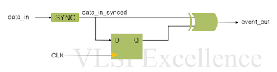
2) The input signal is synchronized to the Event Detector logic domain -
Note:
- When data_in is generated from a different clock domain than 'CLK', a synchronizer (e.g standard 2 -DFF ) is used to synchronize the data_in in the 'CLK' clock domain
- The event_out will get delayed by 2 clock cycles in this case
Waveform :

Please feel free to like/share and comment for any doubts/clarifications regarding Event Detector circuit design.
---------------------------------------------------------Happy Learning --------------------------------


Comments
Post a Comment