Digital Circuit Design - Problem#1
Problem : Design a digital circuit as depicted in below block diagram which takes DIN as an input and runs at a clock speed of CLK and generates an output DATA as shown in the waveform below.


Solution :
- Since the circuit sample the data at both positive and negative edge of the clock, we need both positive edge and negative edge triggered flip-flops
- Lets have a look at below diagram -

- We notice here that by using both positive and negative edge triggered flip-flops, we are able to sample the DIN at both the clock edges but how will we transfer this sampled data to DATA output port ?
- Well, we need to use a 2*1 MUX to select the sampled data from both of the flip-flops but what should be the select signal of this MUX ?
- The select signal should be like the CLK signal
- Lets have a look at below circuit diagram and see if it can produce a select signal which toggles at CLK frequency
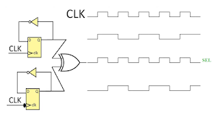
- Yes , here the generated SEL signal can be tied to SEL pin of 2*1 MUX and the MUX output should be similar to the waveform mentioned in the problem.
Hope, this problem helps to understand on how you can design a circuit with given specifications.
Please like/share and comment if you have any doubts related to this problem.
---------------------------------------------Happy Learning --------------------------------------------


Comments
Post a Comment